Hi guys!
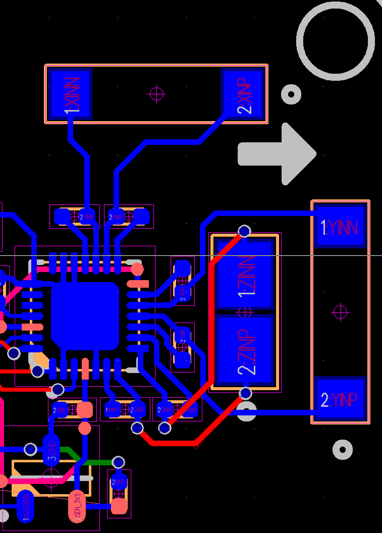
Recently, I designed a new uavcan compass, based on cuav gps hwedef file, everything works, But No matter waht I do, there always a compass inconsistant error,here is the sensors direction,
Hi dave, RM3100.zip (389.9 KB)
of course, I upload the PCB and schematic’s PDF, because It’s designed by orcad and pads, Let me know if you need the source file
im using kicad or Eagle cad for design pcbs… i will check asap.
As i saw the pcb it’s not GND,…
just send me pls all files so checking the board and make some modifications
Yes, That is on purpose, I build this board several times, according to RM3100 datasheet and the breakout board, The best way to handle the Magnetic sensor’s board layout is don’t put any copper under the sensors, It will reduce the interference. and I do test it serval times, If there is a power plane under the sensors, the calibration offsets is much more big than none copper’s version
If you will add GND to your board pcb will not suffer the magnetic field due the current that across the pcb…, ground plane will also dissipate the heat
When you solder it on the pads just add few solder pads…, just use the stencil for apply solder paste.
Too much solder paste can give you interferences…
Do you mind pls attach all the files?
Thank you so much to review my PCB design, I think I find the reason, The AP_Periph and arducopter’s are fine, The reason is RM3100 Z sensors polarity indicator is negative, and the XY sensors are positive. So I solder it wrong at the first place, and the strange thing is, I bought a RM3100 module from the other local guy, he make this mistake too. The PCB does have a small problem, The RM3100 XY sensor’s decal is little bit big, which make the solder much more hard, I will fix it on next version, and Thank you again for help me.
Good… don’t forget to GND the top and the bottom of your pcb. Dont make it power plane but only ground plane… its usefull for dissipate the heat and adding GND vias you don’t need add routes for connect GND pads coz your board is already GND.
GND vias must be place near the pad you need make negative.
Just in case you need a review of the new pcb i will be happy to share info with you
Good day, i cannot open the file and also i cannot convert it.
Ive saw you have add a power plane on your board… i suggest you to make the board ground plane on the top and bottom and remove the power plane in the layer you set it from the layer.
Can you check pls if you can convert it for kicad?
ok,I’ll upload this later, It’s 1am in my timezone now and I change the design little bit base on the rm3100’s datasheet, and we’re tuning a large coper recdntly, which is driver crazy…
 The PCB does have a small problem, The RM3100 XY sensor’s decal is little bit big, which make the solder much more hard, I will fix it on next version, and Thank you again for help me.
 and I change the design little bit base on the rm3100’s datasheet, and we’re tuning a large coper recdntly, which is driver crazy…