Unfortunally the SDA pad unsolderd from hi tempreture of my soldering gun. Is any solution to solder again th SDA pad? Check the photo.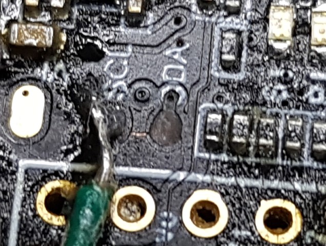
I have one of those boards sitting on the bench. It would be a tedious solder job, like the SDA pin is anyway, but you can try to make the connection as shown. The Baro it’s next to is on the I2C bus but in any case I probed it and it looks good. According to the Hwdef file the process pin PB7 should be good also but I think I would try to solder here instead. Cover the baro vent hole with tape before proceeding 
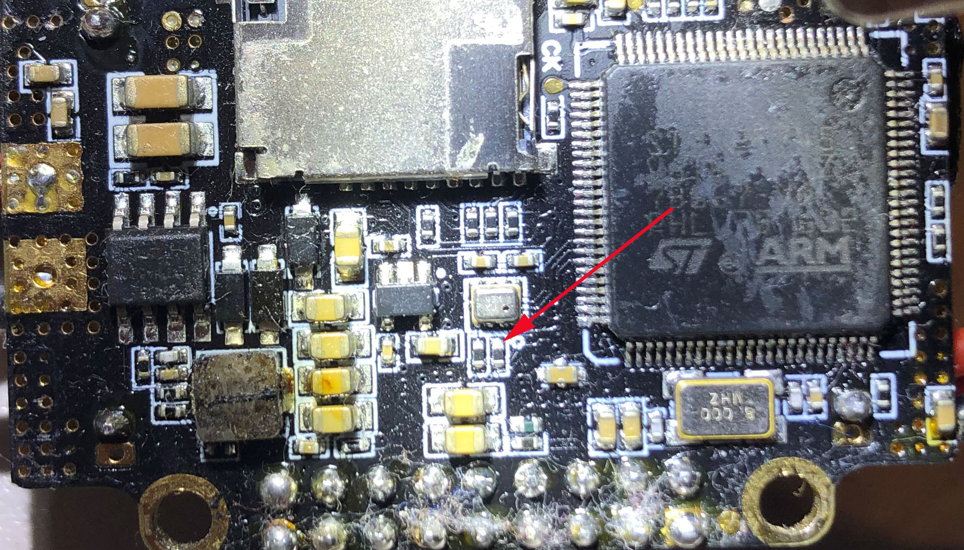
Wow!!! Thank you very very much dkemxr Dave. I"ll give it a try!!! But i’m wondering maybe it’s a way to bridge it without to turn it upside down because is everything soldered tide and it’s gonna be more difficult. Where is pin PB7 by the way?
Here is a link to the processor, check it out.
https://www.st.com/resource/en/datasheet/stm32f745ie.pdf
Ok!! Thank you again dkmxr Dave!!!
Those I2C pads are ridiculously small. After I soldered wires on I put a blob of hot glue over them which seems to have worked well. This FC survived a crash that totally obliterated the Plane it was in and it’s still good!
I see. I check the pdf file and i understand what do you ment. Unfortunally i have to unsolder allmost everything and flip around the board to solder the point you show me near the baro. Thanks for your instractions and your solidarity!!!
Yes, I understand. I probed around on the side the SDA pad is on but I think it routes right thru to the other side as I didn’t find any devices with continuity to the pad. More work it sounds like but hopefully the board will be functional!
Yes,that i expecting at the end,to be functional.I am grateful dkemxr Dave!!!