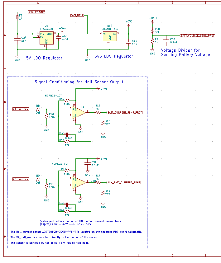
The whole schematic is quite large (this same board is also a CUBE carrier) so I will just post a screen shot of the relevant area.
To help you picture what is going on here: there are actually two stacked PCBs, one contains all the small components that needed narrow, dense traces, and the other (PDB) contains the hall effect current sensor, safety cut off MOSFETS, with thicker copper. The appropriate signals are connected with stackable headers between them.
So, the actual current sensor is on the PDB (and a single decoupling cap), whereas the other components such as LDO and OPAMP, …ect, is on the carrier board.
Here is most of the support components for the current sensor (and a few nonrelated things, hence the 3v3 regulator)
Keep in mind there are two current sensors in my design, so you only need one OPAMP per sensor.
BATT_CURRENT_SENS_PROT and AUX_BATT_CURRENT_SENS connect directly to the CUBEs inputs of the same name (the normal ones you would use with any external sensor)
And here is where the current sensor itself is connected:
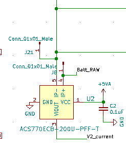
IP+ is directly connected to the battery, IP- is the downstream side of the sensor. V2_current is directly connected to V2_Hall_raw on the other PCB.
Also, if you wish direct message me your email, and I can send you the entire KiCad project if you want to poke around and get ideas. We are open sourcing the design but haven’t settled on a license yet. Once we do, I can post it publicly on the forum.
In case you can’t really see what’s going on, here are PDFs of those pages:
PDB.pdf (64.8 KB)
PowerSense_conditioning-PowerSense_conditioning.pdf (66.6 KB)